l Introduction In the scientific research, production and people's daily life, analog measurement and control are common. In order to measure and control physical quantities such as temperature, pressure, flow rate, speed, displacement, and the like, the above physical quantity is converted into an electrical signal that can simulate a physical quantity through a sensor, that is, an analog electrical signal, and the analog electrical signal is processed and converted into a computer-recognizable one. Digital quantity, sent to the computer, this is data acquisition.
The main problem of data acquisition is the acquisition speed and accuracy. The acquisition speed is mainly related to sampling frequency, A/D conversion speed and other factors, and the acquisition accuracy is mainly related to the number of bits of the A/D converter. The design of high-speed data acquisition system needs to solve the system's contradiction in speed, accuracy, data storage and other aspects.
2. Structure of Data Acquisition System The data acquisition system introduced in this paper uses Samsung's S3C2410 microprocessor. Data acquisition system can be divided into the following parts according to the function: Analog signal conditioning circuit, analog-to-digital converter, data acquisition and storage, clock circuit and system timing and logic circuit, as shown in Figure 1.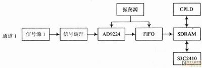
3. Analysis of key technologies of data acquisition system 3.1 System clock circuit design The stability of the clock signal determines the performance of the sampling system. Phase noise and phase jitter are the two main indicators that reflect the stability of the clock. Phase noise describes the spectral purity of the clock signal. Phase jitter directly affects the zero crossing of the clock. High-speed AD sampling systems typically use three clock sources: phase-locked loops, crystal oscillators, and analog mixers. Since once the phase-locked loop loses the reference frequency, the output frequency will immediately jump back to the frequency of the oscillator itself. In addition, when the frequency is adjusted, the output frequency will produce jitter. The larger the frequency difference, the greater the jitter will be. This is disadvantageous and the high speed AD sampling. system. Analog mixers are slow and are only suitable for operation at low frequencies. Therefore, in the design of a high-speed circuit, a high-frequency crystal oscillator is generally selected as a clock source.
In high-speed AD sampling systems, the stability of the sampling clock is closely related to the performance of the SNR. Any clock signal noise and phase jitter of the clock signal will affect the accuracy of the sampling system. The influence of the phase jitter of the clock signal on the SNR of the analog-to-digital conversion can be calculated by the formula:
Where: fs is the sampling clock frequency, N is the number of ADC bits, and Δclk is the amount of phase jitter of the clock signal.
3.2 ADC selection ADC selection In addition to considering data output levels, interface modes, control timing, reference sources, bandwidth and other factors, the most important is to calculate the dynamic index based on design requirements: signal to noise ratio, sampling Rate, full-scale range, etc., so that you can get the ADC's number of bits, the maximum clock frequency, analog input range and other parameters, not only select the required ADC. This design is based on the requirements: sampling frequency 20MHz, real-time sampling 20Msps, the number of digits 12 bits, select the AD9224 chip AD company.
3.3 Analog Signal Conditioning Circuit Design The sampled signal is input into the input channel after low-noise amplification, filtering, etc., of the analog signal conditioning circuit. Since the input signals of high-speed data acquisition systems are mostly high-frequency signals, impedance matching and pre-amplification are required. Therefore, high-speed, low-noise signal preamplifiers and signal transformers can be selected.
The advantage of the signal preamplifier is that the amplification factor is variable and the dynamic range of the signal input is large. It can also be configured as an active filter, but the maximum operating frequency and operating bandwidth of the amplifier must meet the needs of the system to avoid signal distortion.
Signal transformer performance is better than the signal amplifier, and the signal distortion is small. However, the signal amplification factor of the signal transformer is fixed, and the amplitude of the input signal is limited.
3.4 Hard double buffering to achieve continuous acquisition and storage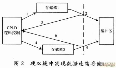
Numbers 1 to 6 in the figure represent the work flow. The acquisition of data is first controlled by the CPLD and written into memory 1 by the FIFO. When the memory 1 data is full, a hardware interrupt signal is generated. This signal has two functions: it informs the microprocessor that the system data has been Ready, by the microprocessor to retrieve data from the memory 1 into the buffer; notify the CPLD control logic to close the data channel between the FIFO and memory 1, and at the same time open the data channel between the FIFO and memory 2, the subsequent data can be continuous without Stored into memory 1 intermittently. At this time, the data of the memory 1 is being read by the microcontroller, and when the data of the memory 2 is ready, a hardware interrupt signal is also generated. This alternate cycle can achieve continuous and no breakpoints in the acquisition of data.
3.5 Multi-channel synchronous acquisition and storage timing analysis To complete the simultaneous storage of multiple signals and continuous data without interruptions and errors, put forward higher requirements on the design of sequential logic. The CPLD devices used in this paper utilize its structure. The features of density, function, speed, and performance, coupled with on-line programmable (ISP) technology, enable accurate timing control and greatly reduce line noise and power consumption.
When multiple signals are latched at the same time, if data is not allowed to be lost, the multi-channel latched data must be stored in the same memory within a single acquisition clock cycle. Suppose that the synchronous sampling frequency is fs, the number of channels is m, and the storage time of each channel is tn (n=1, 2, 3,..., M), then there is t1+t2+t3+...+tm−1/fs, both The sum of all channel storage times is the sampling period.
Assuming that t1=t2=...=tm=T, the conditions for the same storage time for each channel are:
From a practical point of view, there are other time consumptions during an acquisition clock cycle, such as hold time and conversion time. Assuming that other time consumption is ta, then:
If the duty ratio of fs is 1:1, according to the actual working condition of the ADC, it can be approximately considered that ta=1/(2*, fs), that is, only half the cycle time in an acquisition cycle is available for storing data. Single channel storage time: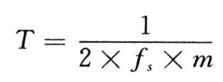
According to the above design, multiple data storage in a single sampling period can be realized.
3.6 System anti-interference design (1) Power supply design According to the theory of high-speed circuit design, the power supply in the AD acquisition system should use a linear power supply to avoid introducing noise into the switching power supply. In order to reduce the impedance of the power supply and reduce the interference of noise on the power supply, power supply layer design is usually used to increase the power supply area as much as possible. When designing the power supply circuit for each chip, decoupling capacitors and bypass capacitors are connected in parallel around the power supply of each chip. Decoupling capacitors provide localized DC for the chip. Bypass capacitors can eliminate high-frequency radiation noise and suppress high-frequency interference.
(2) Grounding technology The analog and digital grounds of the high-speed data acquisition system should be strictly separated and the final single point common ground. The common location usually selects the location where the current required by the ADC chip pin is the largest, so that the large current can be returned to the ground nearest to avoid interference with the analog circuit and improve the system acquisition accuracy.
The analog ground and the digital ground can be connected by magnetic beads. Since the high frequency impedance of the magnetic beads is large and the DC resistance is zero, high-frequency current can be filtered to reduce the high-frequency noise on the ground.
4. Conclusion The high-speed data acquisition system has always been a research hotspot in the field of measurement and control. This article is based on the structure of the ARM9 high-speed data acquisition system and discusses in detail the design of the system clock circuit, the selection of analog-to-digital converters, and the design of analog signal conditioning circuits. Hard double-buffering implements key technologies such as sequential acquisition, multi-channel simultaneous acquisition and storage, and system anti-jamming design. It has been proved that the efficiency of this design scheme is very high.
The problem of anti-jamming in high-speed data acquisition systems is far greater than that in low- and medium-speed systems, such as delays, reflections, crosstalk, excessive internal interference, thermal noise, power supply interference, and ground noise on signal connections. It affects the precision of analog devices such as operational amplifiers and analog-to-digital converters. When the device is serious, the system will not work properly. Therefore, in the design of high-speed data acquisition systems, the acquisition accuracy of the entire system mainly depends on the anti-jamming design of the system. Various measures must be taken during the initial stages of circuit design and board making to reduce or eliminate possible sources of interference. This article mainly considers from the following aspects:
In the high-speed data acquisition process, data storage and S3C2410 read data are required to be performed at the same time. In the related literature, a storage technology based on the double buffering mode of the software system is proposed, but after analysis, it is found that it solves both continuous storage and readings. Reduces the performance of the microprocessor. The hardware-based double buffering mode proposed in this design can solve this problem well. The working principle is shown in Figure 2.
The main problem of data acquisition is the acquisition speed and accuracy. The acquisition speed is mainly related to sampling frequency, A/D conversion speed and other factors, and the acquisition accuracy is mainly related to the number of bits of the A/D converter. The design of high-speed data acquisition system needs to solve the system's contradiction in speed, accuracy, data storage and other aspects.
2. Structure of Data Acquisition System The data acquisition system introduced in this paper uses Samsung's S3C2410 microprocessor. Data acquisition system can be divided into the following parts according to the function: Analog signal conditioning circuit, analog-to-digital converter, data acquisition and storage, clock circuit and system timing and logic circuit, as shown in Figure 1.

Figure 1 Data Acquisition System Structure
3. Analysis of key technologies of data acquisition system 3.1 System clock circuit design The stability of the clock signal determines the performance of the sampling system. Phase noise and phase jitter are the two main indicators that reflect the stability of the clock. Phase noise describes the spectral purity of the clock signal. Phase jitter directly affects the zero crossing of the clock. High-speed AD sampling systems typically use three clock sources: phase-locked loops, crystal oscillators, and analog mixers. Since once the phase-locked loop loses the reference frequency, the output frequency will immediately jump back to the frequency of the oscillator itself. In addition, when the frequency is adjusted, the output frequency will produce jitter. The larger the frequency difference, the greater the jitter will be. This is disadvantageous and the high speed AD sampling. system. Analog mixers are slow and are only suitable for operation at low frequencies. Therefore, in the design of a high-speed circuit, a high-frequency crystal oscillator is generally selected as a clock source.
In high-speed AD sampling systems, the stability of the sampling clock is closely related to the performance of the SNR. Any clock signal noise and phase jitter of the clock signal will affect the accuracy of the sampling system. The influence of the phase jitter of the clock signal on the SNR of the analog-to-digital conversion can be calculated by the formula:
Where: fs is the sampling clock frequency, N is the number of ADC bits, and Δclk is the amount of phase jitter of the clock signal.
3.2 ADC selection ADC selection In addition to considering data output levels, interface modes, control timing, reference sources, bandwidth and other factors, the most important is to calculate the dynamic index based on design requirements: signal to noise ratio, sampling Rate, full-scale range, etc., so that you can get the ADC's number of bits, the maximum clock frequency, analog input range and other parameters, not only select the required ADC. This design is based on the requirements: sampling frequency 20MHz, real-time sampling 20Msps, the number of digits 12 bits, select the AD9224 chip AD company.
3.3 Analog Signal Conditioning Circuit Design The sampled signal is input into the input channel after low-noise amplification, filtering, etc., of the analog signal conditioning circuit. Since the input signals of high-speed data acquisition systems are mostly high-frequency signals, impedance matching and pre-amplification are required. Therefore, high-speed, low-noise signal preamplifiers and signal transformers can be selected.
The advantage of the signal preamplifier is that the amplification factor is variable and the dynamic range of the signal input is large. It can also be configured as an active filter, but the maximum operating frequency and operating bandwidth of the amplifier must meet the needs of the system to avoid signal distortion.
Signal transformer performance is better than the signal amplifier, and the signal distortion is small. However, the signal amplification factor of the signal transformer is fixed, and the amplitude of the input signal is limited.
3.4 Hard double buffering to achieve continuous acquisition and storage

Numbers 1 to 6 in the figure represent the work flow. The acquisition of data is first controlled by the CPLD and written into memory 1 by the FIFO. When the memory 1 data is full, a hardware interrupt signal is generated. This signal has two functions: it informs the microprocessor that the system data has been Ready, by the microprocessor to retrieve data from the memory 1 into the buffer; notify the CPLD control logic to close the data channel between the FIFO and memory 1, and at the same time open the data channel between the FIFO and memory 2, the subsequent data can be continuous without Stored into memory 1 intermittently. At this time, the data of the memory 1 is being read by the microcontroller, and when the data of the memory 2 is ready, a hardware interrupt signal is also generated. This alternate cycle can achieve continuous and no breakpoints in the acquisition of data.
3.5 Multi-channel synchronous acquisition and storage timing analysis To complete the simultaneous storage of multiple signals and continuous data without interruptions and errors, put forward higher requirements on the design of sequential logic. The CPLD devices used in this paper utilize its structure. The features of density, function, speed, and performance, coupled with on-line programmable (ISP) technology, enable accurate timing control and greatly reduce line noise and power consumption.
When multiple signals are latched at the same time, if data is not allowed to be lost, the multi-channel latched data must be stored in the same memory within a single acquisition clock cycle. Suppose that the synchronous sampling frequency is fs, the number of channels is m, and the storage time of each channel is tn (n=1, 2, 3,..., M), then there is t1+t2+t3+...+tm−1/fs, both The sum of all channel storage times is the sampling period.
Assuming that t1=t2=...=tm=T, the conditions for the same storage time for each channel are:

From a practical point of view, there are other time consumptions during an acquisition clock cycle, such as hold time and conversion time. Assuming that other time consumption is ta, then:

If the duty ratio of fs is 1:1, according to the actual working condition of the ADC, it can be approximately considered that ta=1/(2*, fs), that is, only half the cycle time in an acquisition cycle is available for storing data. Single channel storage time:

According to the above design, multiple data storage in a single sampling period can be realized.
3.6 System anti-interference design (1) Power supply design According to the theory of high-speed circuit design, the power supply in the AD acquisition system should use a linear power supply to avoid introducing noise into the switching power supply. In order to reduce the impedance of the power supply and reduce the interference of noise on the power supply, power supply layer design is usually used to increase the power supply area as much as possible. When designing the power supply circuit for each chip, decoupling capacitors and bypass capacitors are connected in parallel around the power supply of each chip. Decoupling capacitors provide localized DC for the chip. Bypass capacitors can eliminate high-frequency radiation noise and suppress high-frequency interference.
(2) Grounding technology The analog and digital grounds of the high-speed data acquisition system should be strictly separated and the final single point common ground. The common location usually selects the location where the current required by the ADC chip pin is the largest, so that the large current can be returned to the ground nearest to avoid interference with the analog circuit and improve the system acquisition accuracy.
The analog ground and the digital ground can be connected by magnetic beads. Since the high frequency impedance of the magnetic beads is large and the DC resistance is zero, high-frequency current can be filtered to reduce the high-frequency noise on the ground.
4. Conclusion The high-speed data acquisition system has always been a research hotspot in the field of measurement and control. This article is based on the structure of the ARM9 high-speed data acquisition system and discusses in detail the design of the system clock circuit, the selection of analog-to-digital converters, and the design of analog signal conditioning circuits. Hard double-buffering implements key technologies such as sequential acquisition, multi-channel simultaneous acquisition and storage, and system anti-jamming design. It has been proved that the efficiency of this design scheme is very high.
The problem of anti-jamming in high-speed data acquisition systems is far greater than that in low- and medium-speed systems, such as delays, reflections, crosstalk, excessive internal interference, thermal noise, power supply interference, and ground noise on signal connections. It affects the precision of analog devices such as operational amplifiers and analog-to-digital converters. When the device is serious, the system will not work properly. Therefore, in the design of high-speed data acquisition systems, the acquisition accuracy of the entire system mainly depends on the anti-jamming design of the system. Various measures must be taken during the initial stages of circuit design and board making to reduce or eliminate possible sources of interference. This article mainly considers from the following aspects:
In the high-speed data acquisition process, data storage and S3C2410 read data are required to be performed at the same time. In the related literature, a storage technology based on the double buffering mode of the software system is proposed, but after analysis, it is found that it solves both continuous storage and readings. Reduces the performance of the microprocessor. The hardware-based double buffering mode proposed in this design can solve this problem well. The working principle is shown in Figure 2.
Stainless Steel Decorative Parts
The stainless steel decorative parts including all the Stainless Steel Parts which for decorative use, like stainless pipe cover, stainless steel Tube end cap, staineless steel connecting joint, stainless steel elbow., etc
Steel Pipe Cap,Stainless Steel Lid,Stainless Steel Cover,Stainless Steel Square Connector
Foshan Dinghan Electrical Technology Co., Ltd , https://www.fsdinghanelectrical.com